


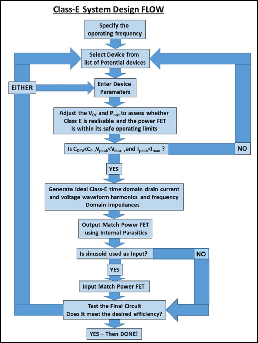

Here we give a brief overview of the results and Design methodology used for the efficiency optimized input & output impedance matched Class-E Power amplifier.
Below is a list of all the topics we cover in this page. Go ahead and click on any of these links, and you’ll be taken to that specific section.
If you would like to know more background information about the Class-E power amplifier and why we designed it, click on button on the right to find out more.
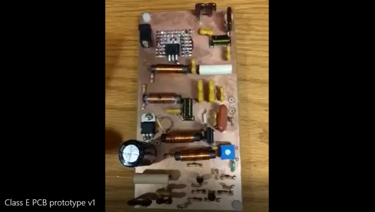
Video showing the top and bottom view of an early version of the Class E PCB prototype.
Class-E Measurement Results
| Measurement | Results |
|---|---|
|
Output Peak voltage |
42Vpeak |
|
Input DC Current |
0.69A |
|
Efficiency (with Vsupply = 36V, Rout = 50Ω) |
71% |
Class-E Simulation Results
| Measurement | Results |
|---|---|
|
Output Power |
17.9W |
|
Input Power |
19.9W |
|
Efficiency |
89.8% |
Step-By-Step Walkthrough Examples:
A quick step-by-step walk-through of the design flow is shown here in Power Electronics of the appendix.
Also a YouTube video demonstrating the design process for the design is provided below.