Maximum Peak Detection and Auto-Tuning Appendix
On this page we give a little more background information for the design as well as the design process used for the Maximum Peak Detection and Auto-Tuning Circuits. For detailed information, click on the button on the right to access the thesis pdf.
Below is a list of all the topics we cover in this page. Click on any of these links to go to that section.
SYSTEM OVERVIEW
Although the MCR-WPT coils system benefits from longer transmission distances compared to other WPT systems, it suffers from a rapid decrease in transmission efficiency when the receiver is located at a distance that is less than the optimal distance away from the transmitter for peak efficiency. This efficiency decrease is due to flux leakage caused by the frequency splitting phenomenon.
A brief explanation of Frequency Splitting and its modes of operations is provided below.
(Note: more information on MCR-WPT coils fundamentals can be found by clicking on the button on the right).
Frequency splitting occurs when multiple coupled resonators form a single system which can oscillate in two modes, one of higher and one of lower frequency than the fundamental frequency, where the frequency separation of the two modes is dependent on the coupling strength between the resonant components. This is due to the mutual inductive coupling between the transmitter and receiver coils being directly proportional to the separation distances between these coils. In other words, when the distance changes, the mutual inductance changes proportionally resulting in the resonant frequency of the MCR-WPT coils system to change and consequently cause the system efficiency to drop at the operational frequency.
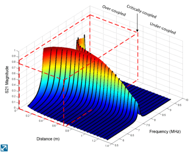
A visual example of frequency splitting can be seen in the region defined by the red dotted line in the image below (image retrieved here↗ ). From the image which shown the S21 as a function of frequency and distance, we can see that the MCR-WPT Coils coupling efficiency can be divided into 3 different modes of operation. These modes are based on the mutual inductive coupling coefficient and are defined as follows:
- Critically-Coupled: This is when the MCR-WPT coil system is at the optimal separation distance. The maximum transmission efficiency of the system occurs at this location.
- Over-Coupled: When the separation distance between the transmitter and the receiver is less than the critical coupling distance (CCD), the efficiency of the system at the operation frequency is reduced, due to frequency splitting. With decreasing separation distance, we get increasing coupling, and increasing frequency separation between the resonant modes.
- Under-Coupled: Beyond the critically-coupled distance, when the separation distance is increased, the coupling between the transmitter and receiver coils is decreased. The system transmission efficiency drops, and it operates in the under-coupled region.
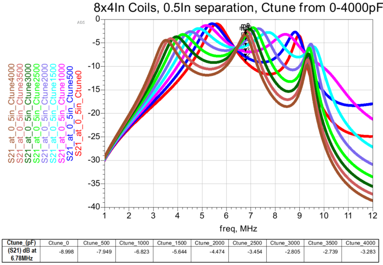
To overcome the effects of frequency splitting and bring back the system into resonance, 3 different tuning methods can be used, namely, inductive tuning, frequency tuning, and capacitive tuning. Inductive tuning can’t be used in our application since the dimensions and/or materials of the coils have to be changed to change the inductance. Also frequency tuning can’t be used because our frequency bandwidth is fixed by the Rezence Standard. Therefore, we are left with capacitance tuning to compensate for the changes in mutual inductance due to distance changes. An example of the tuning results for capacitance tuning on a MCR-WPT coils system in the over-coupled region is shown in the image below.
From the image, when the MCR-WPT coils are close at separation distances of 0.5 inch, it can be seen when Ctune is 0pF, the frequency splitting is significant. By incrementally increasing the Ctune capacitance value, the resulting S21 values represented by the markers were placed on plots for each value Ctune at the 6.78MHz operating frequency, we steadily improve the efficiency. Near 3.5nF the system is brought back into resonance and get the maximum S21 value.
For more information on the basic Frequency Splitting Theory, and MCR-WPT coil capacitive tuning, check out section 4.1.1 and 4.1.3. of the thesis. For more brief overview of the Rezence WPT standard, see section 1.1.1 The thesis can be obtained from the Ryerson University library by clicking the button below.
MAXIMUM PEAK VOLTAGE DETECTION PROCESS
We used the following method to detect when the maximum tuning peak is achieved, and determine the separation distance tuning range as described below:
- The expected maximum tuned output peak voltage (Vm) is known for different distances.
- The sum of the comparator, AND-Gate and counter propagation delays (tPDeq) is known.
- Comparator threshold voltage (VTH) and the rectifier diode voltage drop (Vrect) are known
- Therefore a close estimate of the required output peak voltage of the Negative Voltage Level shifter voltage (Vfeq) for tuning shut off can be calculated using the equation below.

Thus for different expected Vm, the resulting distance tuning ranges are shown below.
MAXIMUM PEAK DETECTION SYSTEM
The Maximum Peak Detection portion of the system is composed of 3 main circuit blocks that perform different functions within the system. In this section we describe the function each of these circuit blocks and identify the key factors that needed to be considered when designing them.
- Negative Voltage Level Shifter
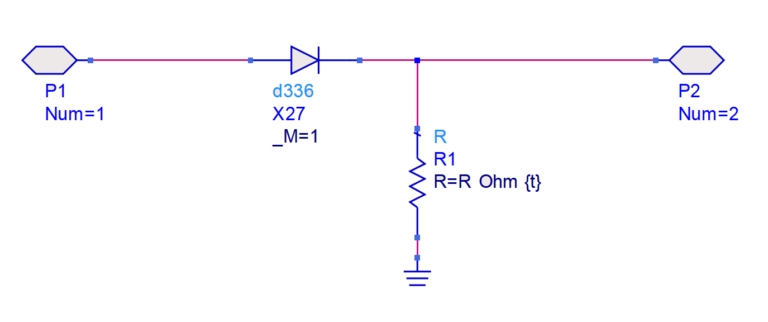
- Half Wave Rectifier
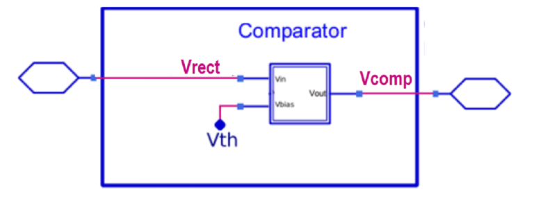
- High Speed Comparator
FUNCTION
- Main function:
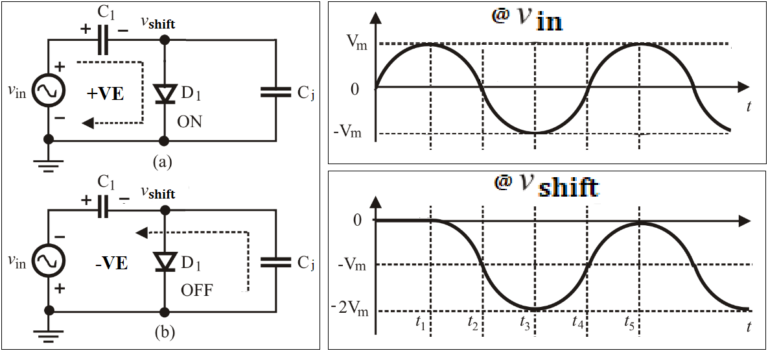
- Shifts the MCR-WPT Coil output voltage signal down, so that the voltage peak can be used for determination of the maximum peak.
KEY DESIGN FACTORS
- C1 ≥ 100 Cj for negligible signal loss
- C1 small to limit setup time
- Vfeq large enough to overcome the Vrect at the rectifier and turn on comparator.
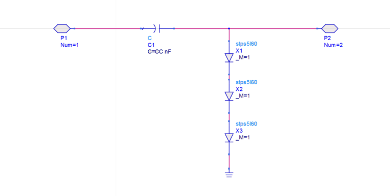
- Multiple diodes in series (as seen below) to reduce C1 capacitance and increase Vfeq
More background information is provided in section 4.2.1.1 and appendix A of the thesis which can be retrieved by clicking respective button below.
FUNCTION
- Main function:
- Ensures that the negative part of the Negative Voltage Level Shifter signal is removed, so that Comparator’s input voltage is within its absolute maximum input voltage ratings at the following stage.
KEY DESIGN FACTORS
- In forward bias, the Vfeq signal is sent to the comparator, therefore:
- Vrect (diode forward voltage drop) < Vfeq such that the comparator can turn on.
- Small diode on resistance (RDSon).
- In reverse bias, acts as high pass filter, therefore:
- Crect (reverse diode capacitance) must be small to ensure the signal is cut off during reverse bias mode.
- Rrect must be small for the same reason, but large enough to ensure low power consumption.
More information is provided in section 4.2.1.2 of the thesis which can be retrieved by clicking respective button below.
FUNCTION
- Two main functions:
- It is used to generate a digital pulse to the input of the auto-tuning circuit.
- Its propagation delay (tPD) is used as part of determining the maximum tuning peak.
KEY DESIGN FACTORS
- Device Selection key parameters:
- Small comparator tPD (load capacitance, temperature, etc affect this value).
- Small Vio(aka VTH) to ensure small current through rectifier.
More information about the comparator’s functional operation within the system is provided in section 4.2.1.3 of the thesis which can be retrieved by clicking respective button below.
AUTO-TUNING SYSTEM
The Auto-Tuning portion of the system is composed of 3 main circuit blocks that perform different functions within the system. In this section we describe the function each of these circuit blocks and identify the key factors that needed to be considered when designing them.
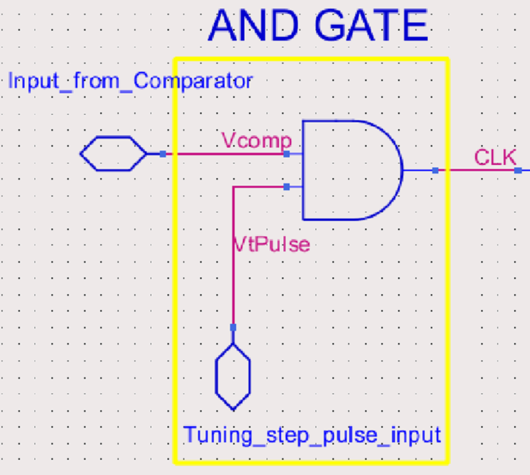
- High Speed AND-Gate
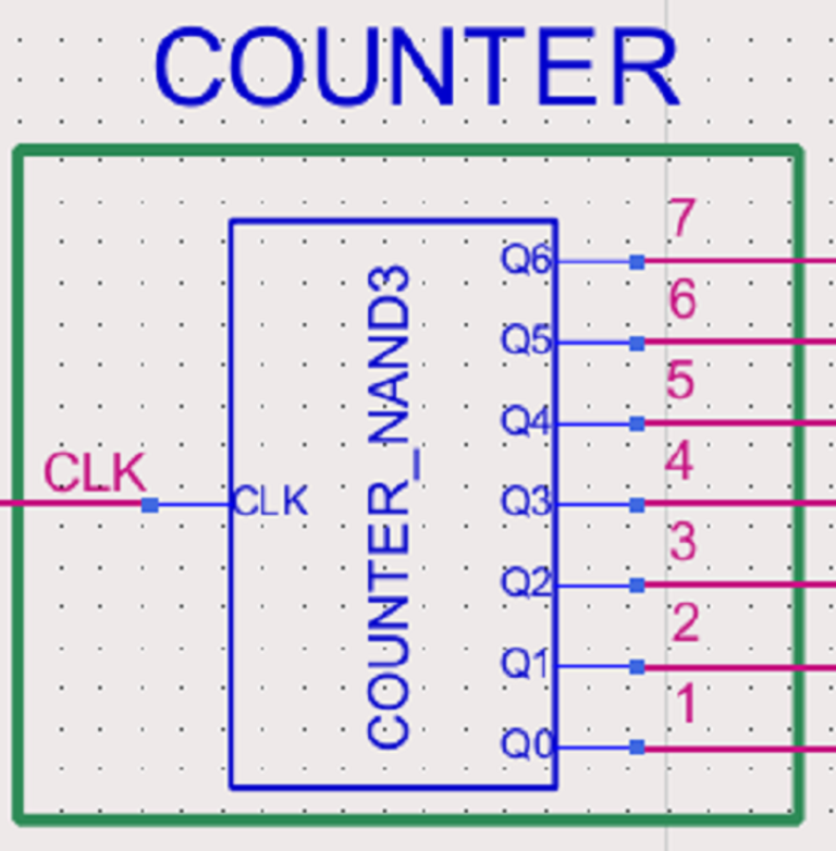
- High Speed Binary Counter
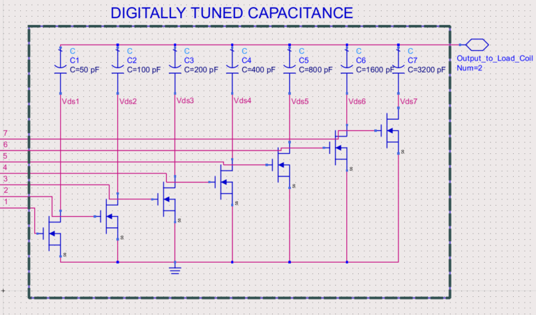
- Digitally Tuned Capacitance
FUNCTION
- Three main functions:
- Delays the auto-tuning circuitry during the initial system setup time to allow enough time for the capacitor in the negative voltage shifter to charge up.
- Controls the periodicity of each tuning step to give each tuning capacitor enough time to charge up after each step.
- Its propagation delay (tPD) is used as part of determining the maximum tuning peak.
KEY DESIGN FACTORS
- Device Selection key parameters:
- Small AND-Gate tPD (load capacitance, temperature, etc affect this value).
More information about the AND-Gate’s functional operation within the system is provided in section 4.2.2.1 of the thesis which can be retrieved by clicking respective button below.
SIDE NOTE:
The AND-Gate and Counter like most modern digital ICs use IBIS behavioral models instead of spice functional models. A hacked counter needed to be created to functionally model the counter’s propagation delay. This is described in paragraph 3 of section 4.3.2.
FUNCTION
- Two main functions:
- Discretely increments the MCR-WPT coils output capacitance at every tuning step.
- Its propagation delay (tPD) is used as part of determining the maximum tuning peak.
KEY DESIGN FACTORS
- Device Selection key parameters:
- Large maximum clock frequency (fmax).
- Inversely proportional to its tPD since only the input clock signal is used.
- Worst case Input transition rise and fall rate (∆t/∆v):
- Value must be slower that the worst case AND-Gate output transition rate.
More information the Digitally Tuned Capacitance’s functional operation within the system is provided in section 4.2.2.2 and appendix D.2 of the thesis which can be retrieved by clicking respective button below.
FUNCTION
- Main function:
- Used to connect the capacitors to the output of the MCR-WPT coils.
KEY DESIGN FACTORS
- Device Selection key parameters:
- Small Gate-Drain Charge (Qg).
- Minimize the MOS switch turn-on time using the counter’s output current.
- Low Static Drain-Source on resistance (RDS(ON)).Reduce power loss.
- Small Input Capacitance (Ciss).
- Less than counter’s maximum load capacitance so that it is not overloaded.
- Small Vio(aka VTH) to ensure small current through rectifier.
More information about the comparator’s functional operation within the system is provided in section 4.2.1.3 of the thesis which can be retrieved by clicking respective button below.
DEVICE LIST & PROTOTYPE LAYOUT
Below is a list of the selected discrete electronic devices used in Maximum Peak Detection and Auto-Tuning Simulations, and their respective Key Device Parameter Values.
STPS5L60
| Key Device Parameter | Value |
| Cj | 100-700pF |
| VR | 60V |
BAS70
| Key Device Parameter | Value |
| Cj | 1-5pF |
| VR | 70V |
| RDS(ON) | 8-250Ω |
AD8561
| Key Device Parameter | Value |
| tPD | 7ns |
| Vio | 7mV |
74LVC1G08
| Key Device Parameter | Value |
| tPD | 4ns |
| ∆t/∆v | 10ns/V |
SN74LV4040A
| Key Device Parameter | Value |
| tPD | 3.5ns |
| ∆t/∆v | 20ns/V |
DMG1029SV
| Key Device Parameter | Value |
| Qg | 0.28nC |
| RDS(ON) | 3Ω |
| Ciss | 42pF |

